Semiconductor Process Equipment Business
Semiconductor Process Equipment Business, manufactures, and sells equipment that ensures process superiority by chemically reacting materials or performing special treatments, based on the principle of "meeting society's expectations with chemistry."
Our Semiconductor Process Equipment includes Wafer Handling System series for three-dimensional packaging, Fan-Out Packaging Equipment (FOWLP and FOPLP), and Resist Ashing Equipment that removes resist by plasma processing. We also offer UV Curing Equipment that improves plasma resistance and heat resistance by reacting photoresist with UV.
-
Wafer Handling System
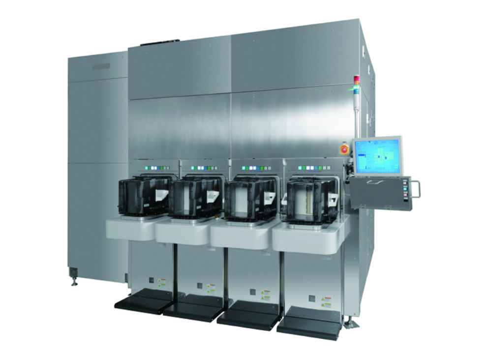
As a solution for advanced packaging, we have developed our own wafer handling system for 3D and 2.5D packaging technology, where wafers are thinned and stacked, and provide equipment for this process.
We also offer provide wafer level (FOWLP) and panel level (FOPLP) equipment for fan-out processes. -
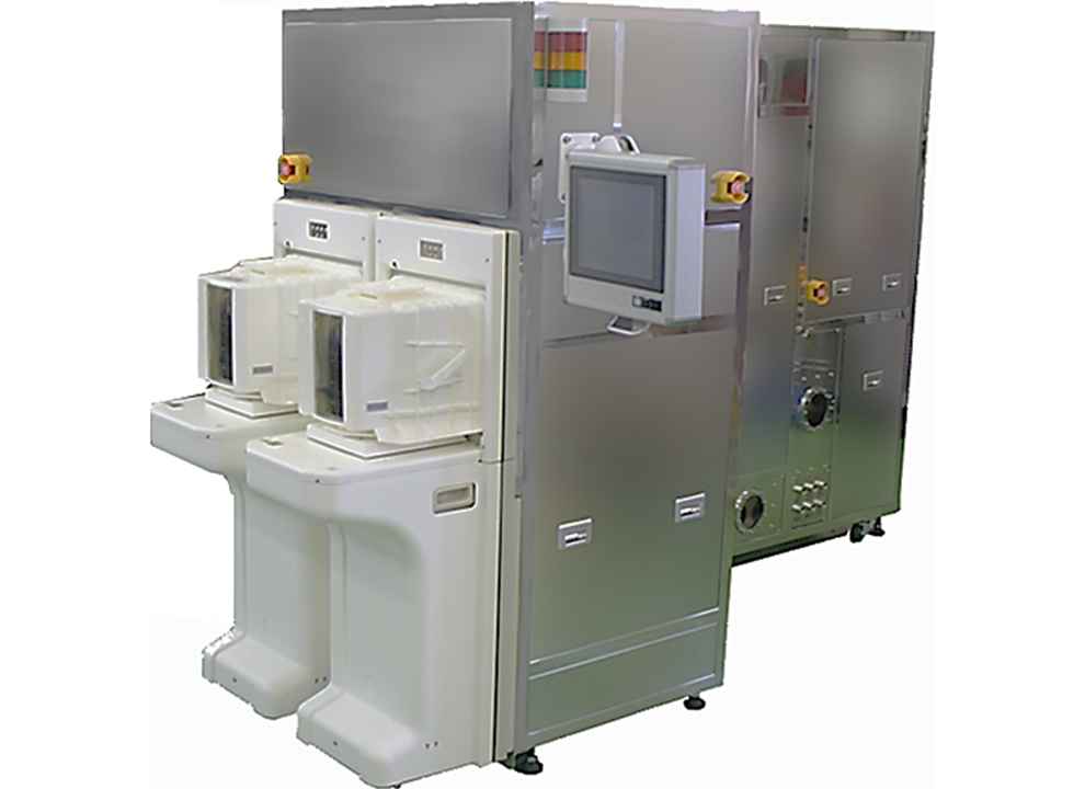
Plasma Ashing Equipment
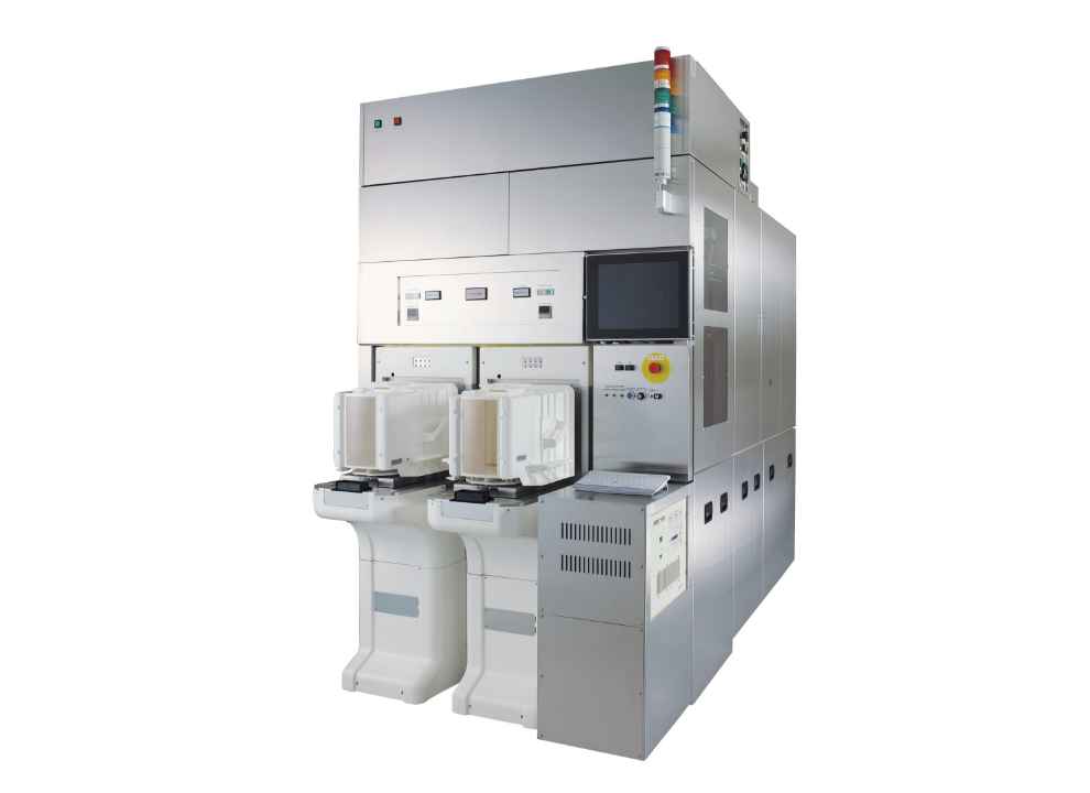
We provide Plasma Ashing Equipment equipped with plasma sources such as comb electrodes, which are standard for post-implantation ashing, and ICP electrodes, which enable damage-free ashing in accordance with various requirements.
We also offer equipment that can handle a wide range of wafer sizes, from 75 to 300mm, and that can transport ultra-thin wafers. -
UV Curing Equipment
We provide equipment that can improve the heat resistance, dry etching resistance, and chemical resistance of any organic thin film.