Equipment for 3D Packaging and Fan-Out Wafer Level Package (FOWLP)
For 3D packaging technology (3D and 2.5D) where wafers are thinned and stacked, we provide equipment for attaching wafers and support glass (TWM12000 series) and equipment for removing and cleaning support glass from thinned wafers (TWR12000 series), These equipment are also applicable to fan-out wafer level packages (FOWLP).
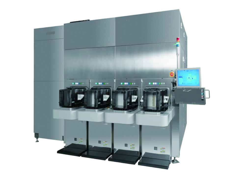
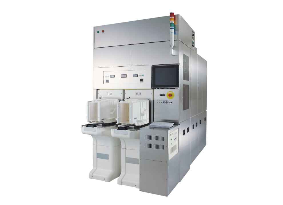
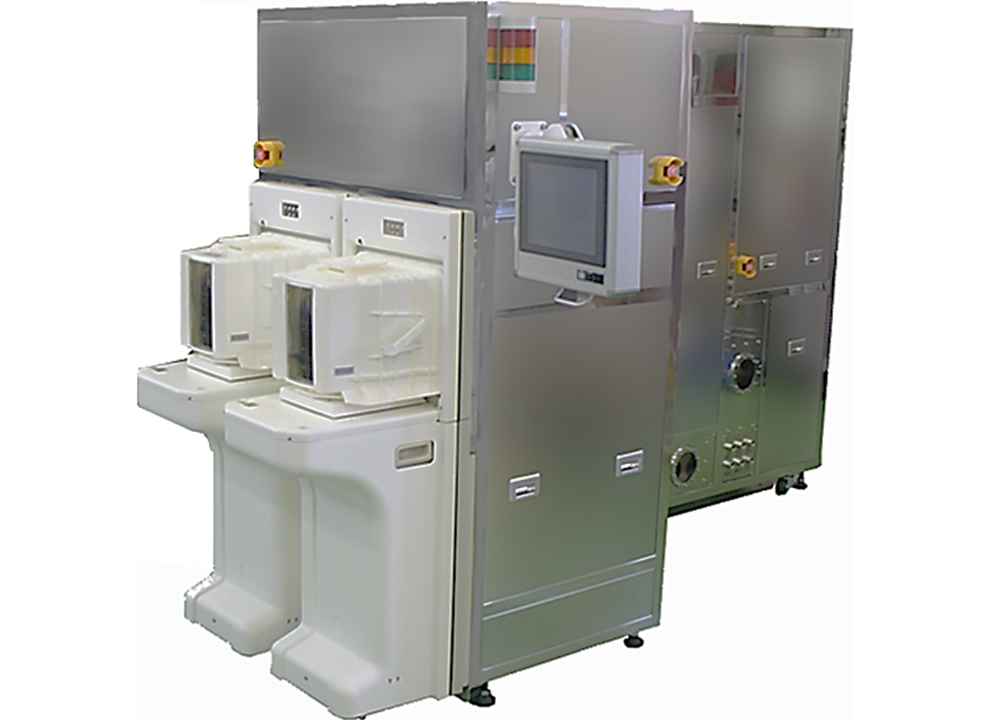
TWM12000 Series Bonder Equipment
Capable of Bonding Bare Silicon and 80μm Bump Substrates With Good Intra-Surface Uniformity
TWM temporary bonding machine is a machine to bond wafers to the support glass using temporary bonding adhesive. This equipment can perform a single step from applying the temporary adhesive to the wafer to attaching it to the support glass. The adhesive can be cleaned with a chemical solution to ensure a residue free cleaning after the process. It is possible to apply up to 10,000cP of temporary adhesive to a substrate with bumps.
Specs
Applicable Wafers
Can be used for 200mm、300mm 300mm⇔200mm
Software
GEM/GEM300
Other Functions
Flip bonding available
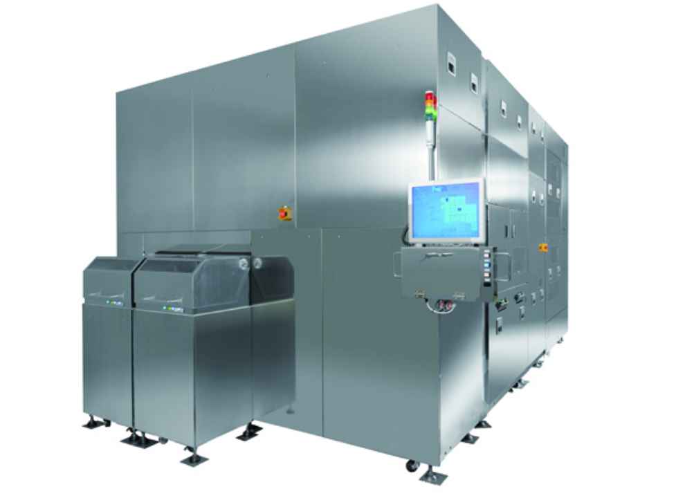
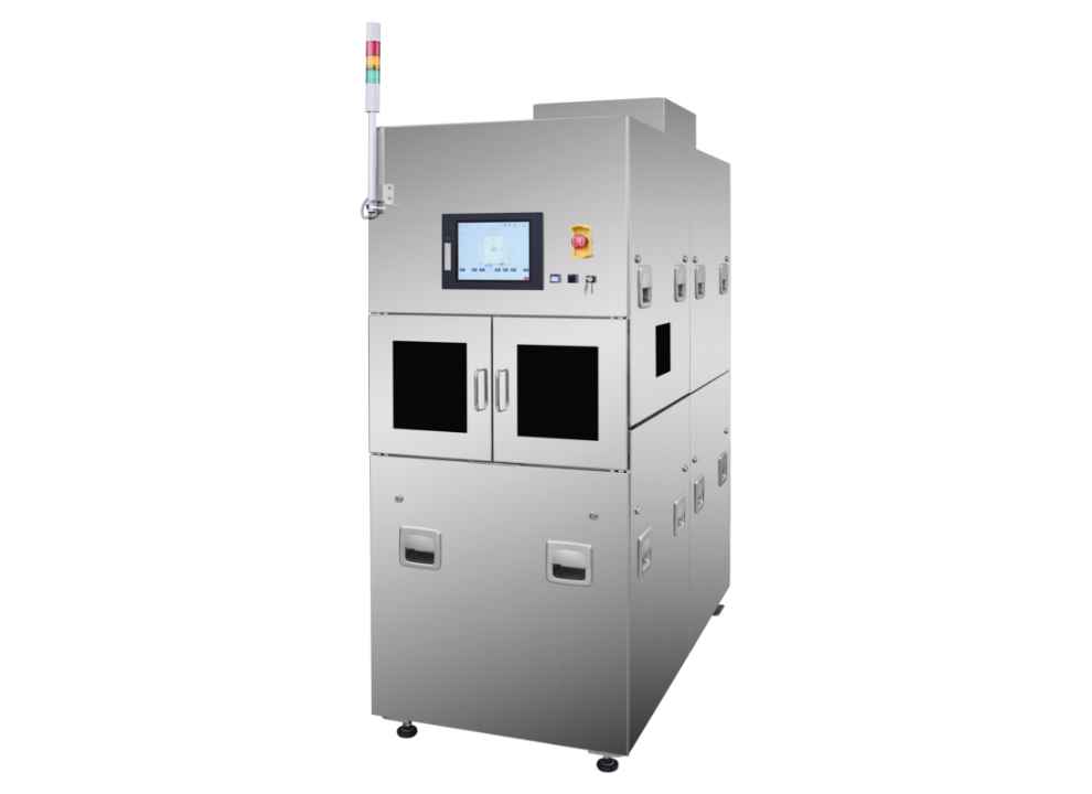
TWR12000 Series Debonder Equipment
Can Remove Glass Without Damaging Device Wafers by Laser Peeling, and Can Clean Bumped Substrates Without Any Residue by Chemical Cleaning
TWR peeling/cleaning system peels off the support glass by laser irradiation and cleans the separation layer and temporary attachment adhesive with special chemicals. When removing the support glass from the substrate, it is possible to do so without damaging the substrate, and the temporary adhesive layer can be cleaned without any residue by cleaning with chemicals. Since we use temporary bonding adhesive that can be cleaned with chemicals, it is possible to clean the bump board without any residue.
Specs
Applicable Wafers
Can be used for 200mm, 300mm, 300mm ⇔ 200mm Compatible with wafer level and dicing frame
Software
GEM300 compatible
Equipment for Fan-Out Panel Level Package (FOPLP)
This is a fan-out panel level package (FOPLP) laminating, peeling and cleaning system for large carriers. FOPLP is a technology that will play a leading role in the next generation, as the 510x515mm size can take up to four times as many chips as a 12-inch wafer, and it can produce large quantities of large-size chips. Based on the technology at the wafer level, we have pioneered the development of FOPLP and provide the laminating, peeling, and cleaning equipment compatible with FOPLP.
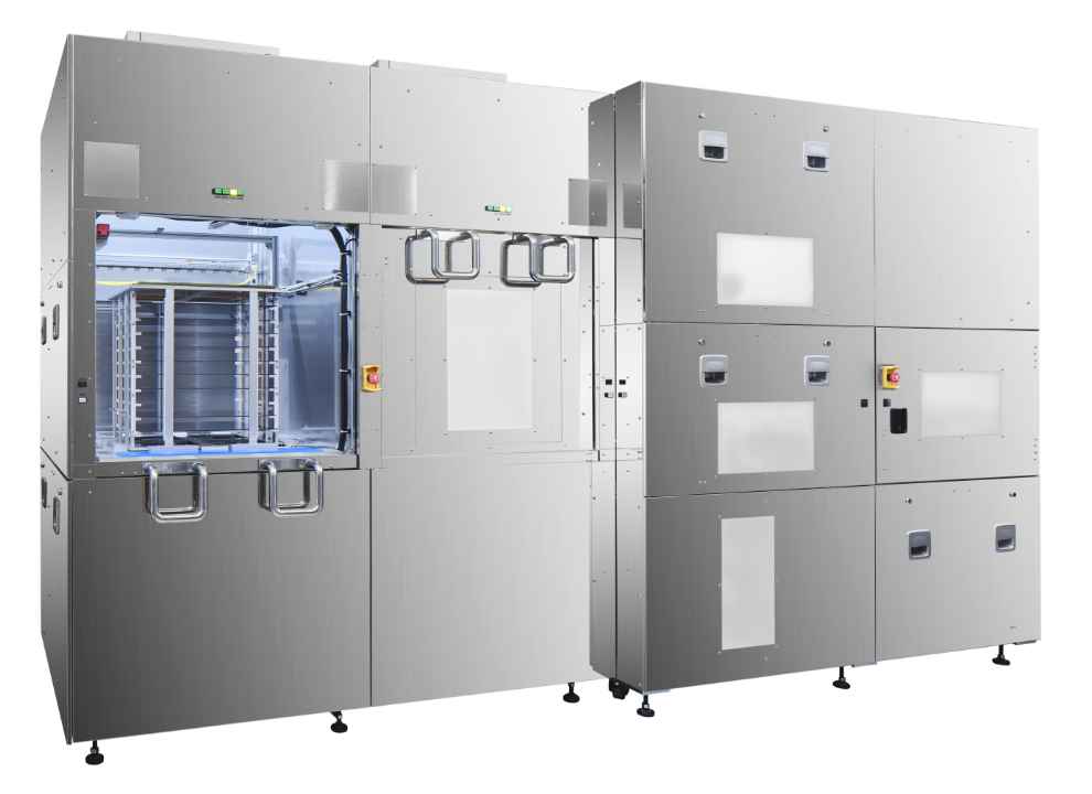
TWM36000 Series Bonder Equipment
Panel Bonding System for Fan-Out Panel Level Packages High-Precision Bonding of Support Glass and Mold Substrate
This series is designed for high-precision bonding of support glass and mold substrate with a release layer and temporary bonding adhesive. The mold substrate is de-watered by vacuum baking prior to attachment, and then attached under vacuum after high precision alignment. Post-application baking is also possible.
Specs
Applicable Substrate Sizes
510×515mm、600×600mm
Equipment Configuration
Bonding unit, vacuum bake, post-bake, pre-alignment unit
Software
GEM300 compatible
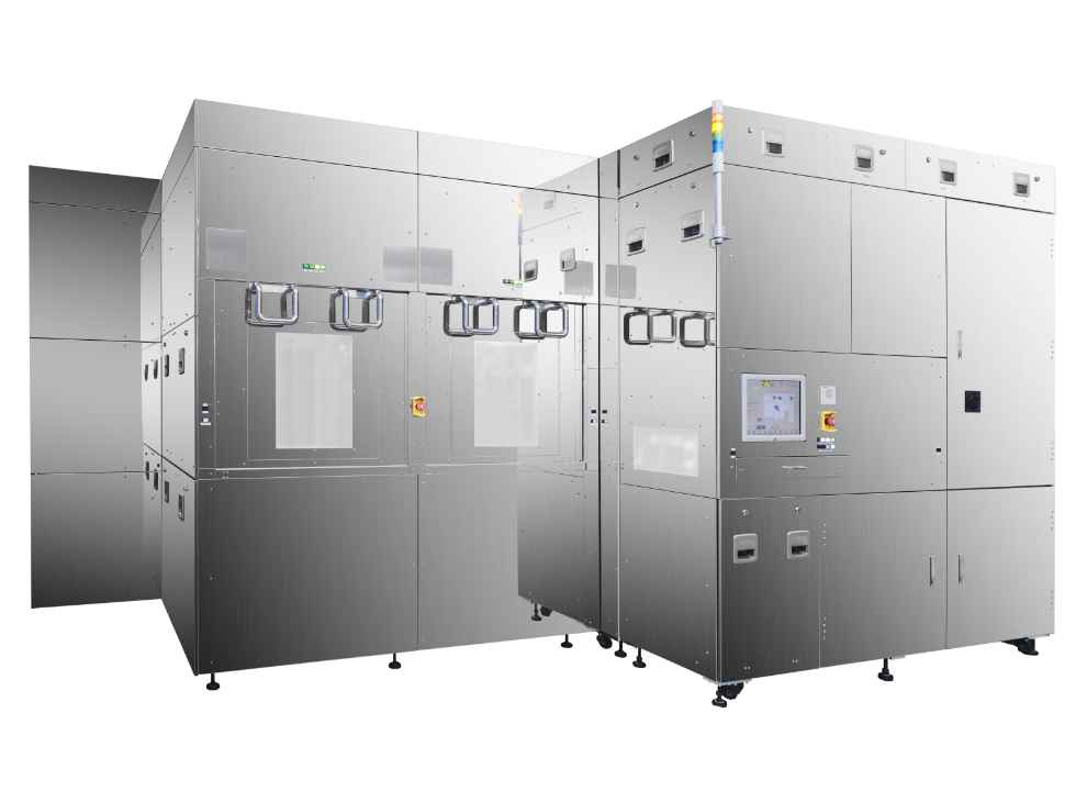
TWR36000 Series Debonder Equipment
Supports Panel Debonding, Cleaner System Fan Out Panel Level Package Single Step System for Removal and Cleaning of Support Glass
This is a system that carries out laser irradiation from the support glass side, peels off the support glass from the mold substrate, and cleans the peeling layer and temporary adhesive on the mold substrate without any residue. The system is also equipped with an ashing device that can be used for dry cleaning, and can also be used to clean the release layer that cannot be dissolved.
Specs
Applicable Substrate Sizes
510×515mm、600×600mm
Equipment Configuration
Laser peeling unit, solvent cleaning cup, ashing unit, flip unit
Software
GEM300 compatible
Plasma Ashing Equipment
TCA-7200/7800 Series
Plasma Ashing System Suitable for Power Semiconductor Manufacturing
This equipment is compatible with 100/125/150/200/300mm wafers. It can perform rapid resist stripping after injection of high-dose ions. It also has a new wafer adsorption mechanism for improved wafer cooling efficiency. Unlike the electrostatic chucking system (ECS), there is no problem with dechucking. It is ideal for ultra-thin wafers such as power semiconductors.
Small-Footprint Resist Ashing System TCA-5800 Series
Small Footprint Asher That Fits Into the Small Space of Older Ashers and Supports Various Ashing Processes
This equipment can be used to replace our older ashers (TCA-2400/3400, TCA-2600/3600, TSE-306W, OAPM-301B-301B). With the same or better process performance, it can be easy to replace older equipment using the existing space. The new controller is equipped with new functions such as equipment status check (leak, operation speed, consumables operation count, etc.) and logging.
Specs
Conveyance System
Air conveyance system 1 chamber, 1 cassette (option: 2 cassettes)
Applicable Wafer Sizes
75mm、100mm、125mm、150mm、200mm
Applicable Processes
Ashing, etching
Processing Chamber
Same as existing process chamber
(TCA/E-2400、TCA/2600、TSE-306W、TCA/E-3400、TCA/E-3600)
Throughput
Equal to or greater than existing equipment
Other Functions
Process log, equipment status check (leak, consumables operation count, operation speed, etc.), logging function
UV Curing System
TIPS-5200/5800 Series
UV Curing System Compatible With G-Line, I-Line, and KrF Resists.
This series is compatible with 100/125/150/200/300mm wafers and is equipped with a wave length modulation system to match the film characteristics. We offer our own UV curing process based on chemical reaction. Even transparent films can be cured without degrading the transmittance. It can also be used for thinner wafers such as power semiconductors.