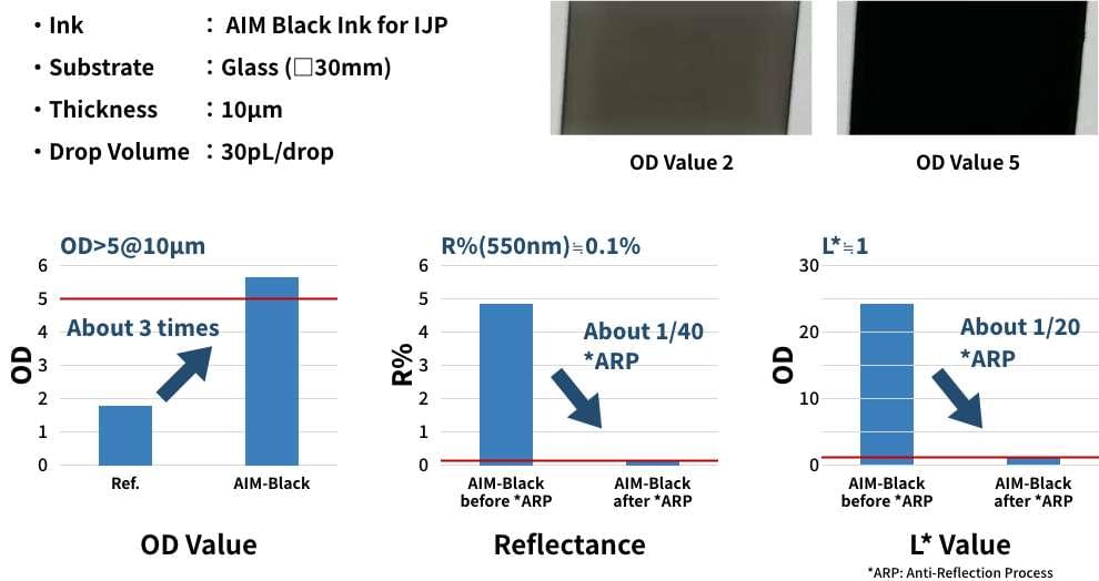
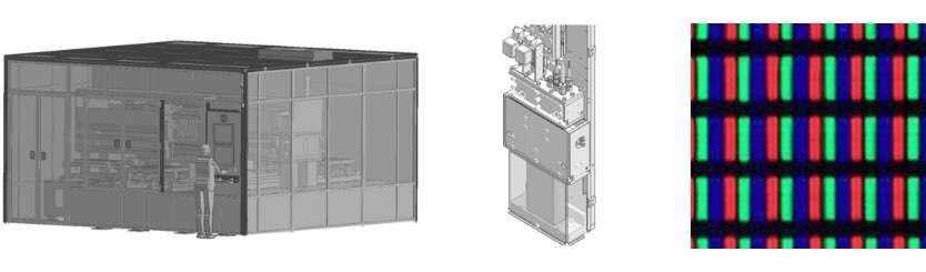
Achieved High Light-shielding Inkjet Deposition Process with >OD 5.
Further Anti-Reflection Process allowed us to achieve Reflectance 0.1% and L*1.
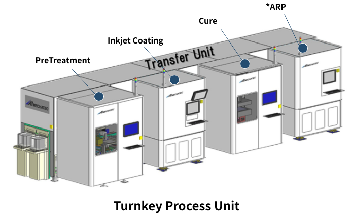
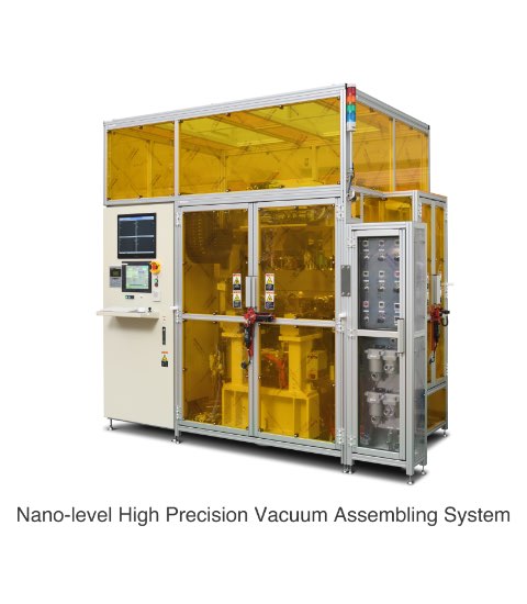
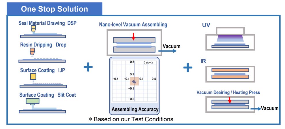
Turnkey Process Solution covering multi-substrates Surface Modification, Coating, and Curing.
Inkjet Process Features
Flexible Form Printing and Unique Thickness Control
Features Standard Material Gradient Coating Capability
Standard Coating Control to suppress Coffee-Stain (Edge)
Application
Display and Micro LED: Black Matrix
For High-Performance Camera Modules, Lenses, and Prisms: Very Low Reflectance and High Light-Blocking Properties
AR/VR: Enhanced Contrast and Reduced Stray Light through Partial Light Shielding
Laser Light Source: High Light Shielding
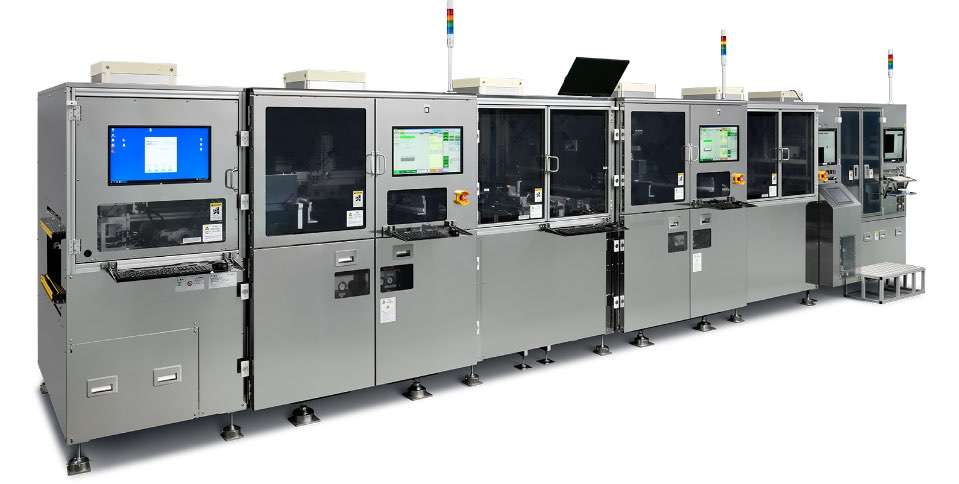
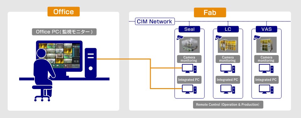
Linear AMC Module Production System
*AMC: Automated Material Connect
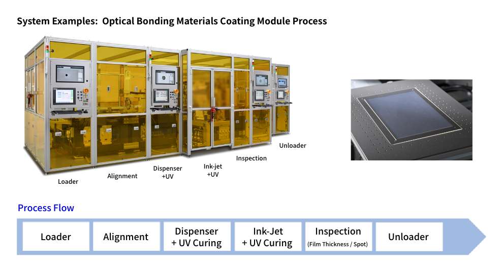
Propose Coating Process for various Resin Materials such as Optical Bonding Materials as One-stop Solution.
Realized Lower Cost Process by optimizing Module Production Process with Circulation Linear Transport System.
Enabled to link with applications such as High-Precision Coating Mechanism like Ink-Jet Printer, Dispenser, etc.
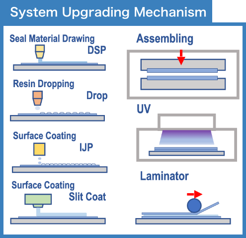
in accordance with the production sites. System Upgrading with Laminator / Assembling Mechanism is possible.
Applications: Module Process for Information Terminals such as Smartphone and Tablet, Information Display Devices such as In-Vehicle Center Information Display, and Various Coating and Assembling Process
Basic Specifications
No.
Items
Specifications
1
Work Size
340mm×250mm
2
Work Materials
Alkali-free Glass / Glass Epoxy
Please inquire for details.
3
Applicable Materials
Optical Bonding Materials, etc.
Please inquire for details.
4
Line Cycle Time
12sec. & over
Varied depending on System Configuration
5
System Upgrading
Refer to System Upgrading Mechanism at the right column.
6
System Size
W8,200 x D3,200 x H2,400mm
Varied depending on System Configuration
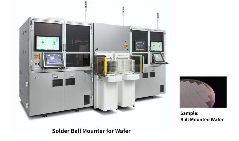
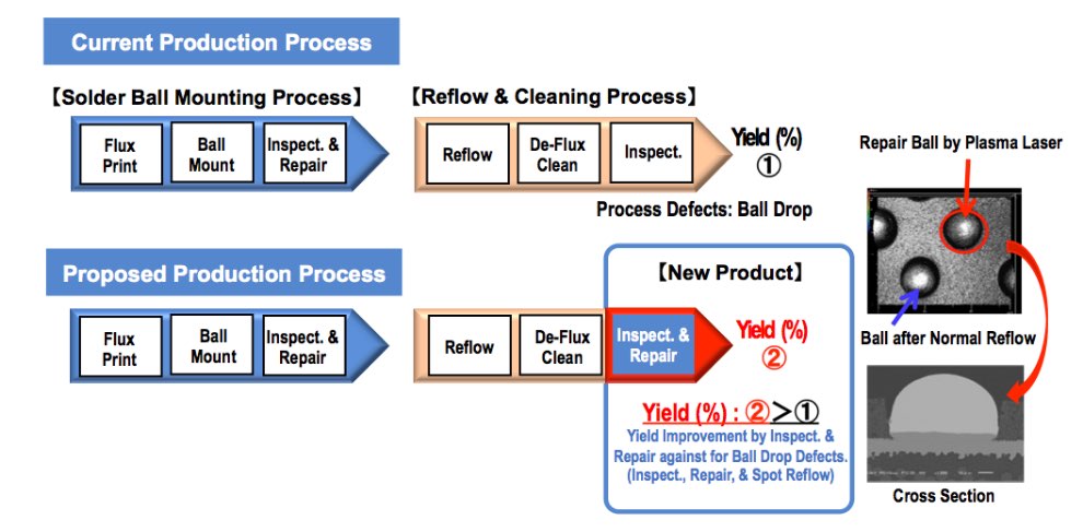
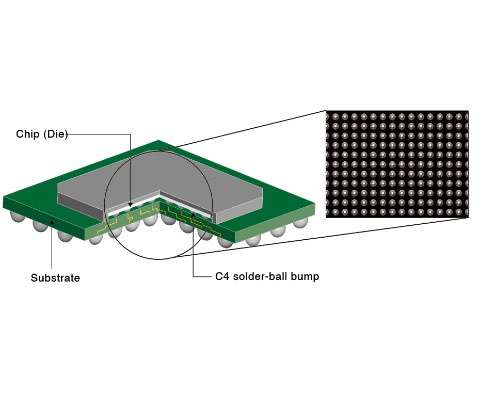
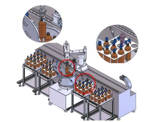
Solder Ball Mounter for Wafer
Realized Higher Yield by applying Ball Mounting Technology for Semiconductor Package Substrate to Wafer
Enabled High Quality & Stable Production by Special Flux Printing Technology
Improved Productivity by New Squeegee Head
Compact Design
Applicable for SECS/GEM, OHT & AGV (Option)
Features
Flux Printing
・Reduced Flux Bleeding by Gap Printing
・Stabled Transfer Position by One-direction Printing Mechanism
・Minimized Cleaning Frequency
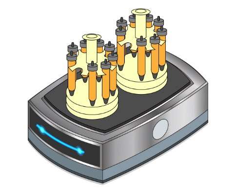
Ball Mounting
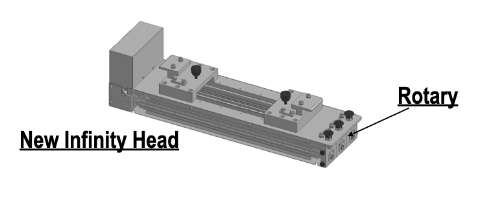
・New Infinity Head (Triple Type Rotary & Closed Type Squeegee)
・Higher Throughput
・Minimized Sweeping Frequency
(1/3 compared with the conventional type)
・ Increased Solder Ball Use Efficiency
(1/2 compared with the conventional type)
・Magnet Adsorption & Snap-Off Mechanism
Application
Wafer such as WLCSP, FOWLP, etc.
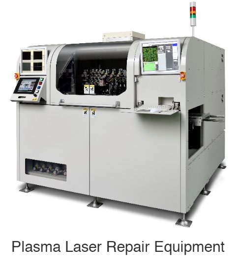
Inspection & Repair
Enabled to systematize Ball Mounting System with Inspection &
Repair Equipment
Specifications
No.
Items
Specifications
ABM-04G-WFS
ABM-04S-WFS
1
Wafer Size
Φ300mm Φ200mm
Φ300mm Φ200mm
2
Handling System
Load port (FOUP or FOSB)
Load port (FOUP or FOSB)
3
Applicable Ball Size
40um~300um
80um~300um
4
Alignment Accuracy
<±10um
<±15um
5
Flux Printing
Gap Printing
(Single Direction)
Gap Printing
(Single Direction)
6
Ball Mounting
Adopted New Infinity Head (Triple Type Rotary & Closed Type
Squeegee)
Adopted New Infinity Head (Triple Type Rotary & Closed Type
Squeegee)
7
Ball Missing Rate
<20ppm (as per AIM’s test conditions)
<30ppm (as per AIM’s test conditions)
8
Throughput
65UPH
(as per AIM’s test conditions)
40UPH
(as per AIM’s test conditions)
9
Equipment Size
3995(W)x2150(D)x2020(H)mm
3555(W)x2150(D)x2020(H)mm
10
Equipment Weight
Approx. 3,500kg
Approx. 3,300kg
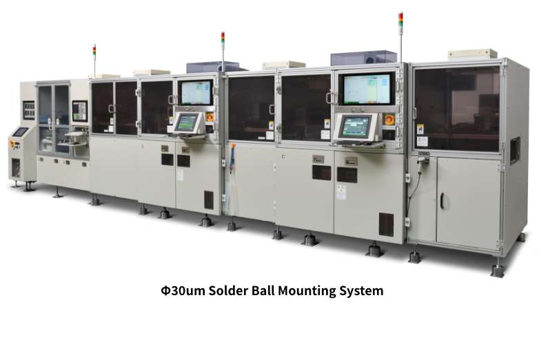
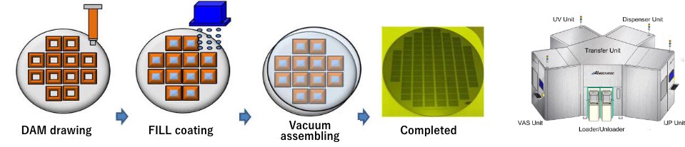
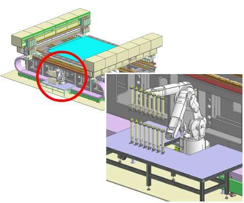
Φ30um Solder Ball Mounting System (Patented)
Realized Uniform Flux Coating enabling Ultra Fine Pitch by Inkjet
Technology.
Contributed to Stable Ball Mounting and Productivity Improvement by
High-Speed Rotary Head.
Enabled High-Speed Inspection and Repair by “On the Fly Inspection” as
Non-Stop Continuous Inspection.
Total Solution contributing to Yield and Productivity Improvement for
Microscopic Solder Ball Mounting Process with Ultra Fine Pitch.
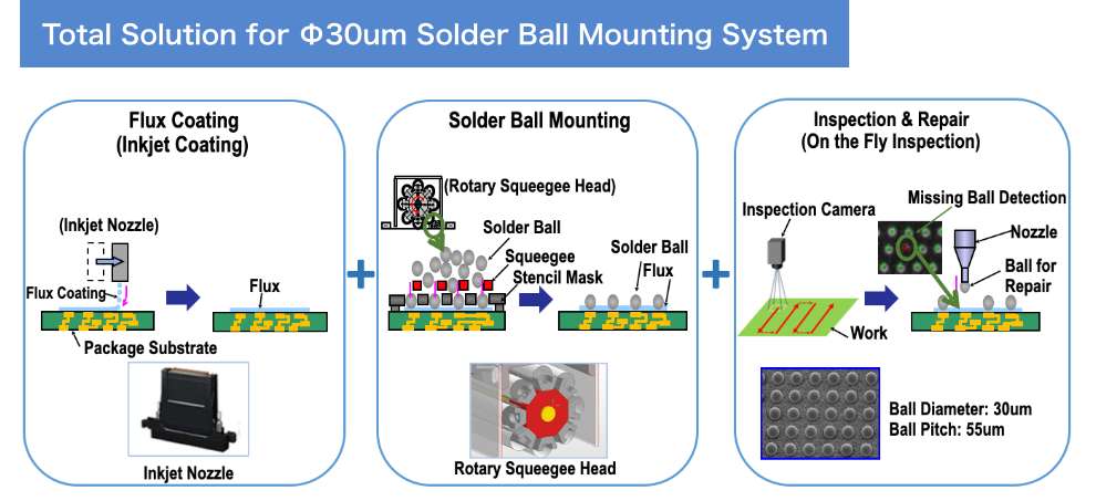
Features
Flux Coating
Inkjet Coating without using conventional Stencil Mask
Ball Mounting
New Rotary Head to provide High Throughput
Inspection & Repair
Continuous High-Speed Inspection (On the Fly)
Capable for □120mm Unit size Inspection & Repair
Not required Stencil mask for Flux printing process and Flux Usage
to be improved